PCB Fabrication at PCBSKY - PowerPoint PPT Presentation
Title:
PCB Fabrication at PCBSKY
Description:
PCBSky offers types of one-stop PCB services from China with its professional PCB manufacturing factory experience. We are a quality PCB,Flex PCB and SMT manufacturer in China, providing full PCB fabrication and assembly services in certified quality standards. – PowerPoint PPT presentation
Number of Views:2
Title: PCB Fabrication at PCBSKY
1
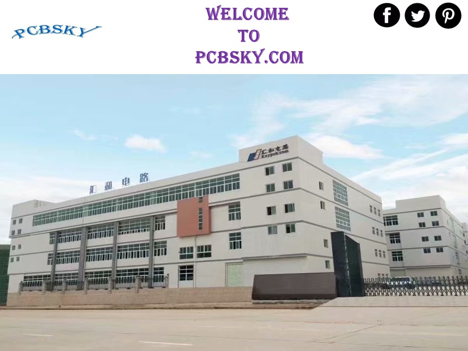
WELCOME TO PCBSKY.COM
2
Conventional PCB
Via in Pad
The holes drilled on the chip pads on the PCB can
be referred to as VIA IN PAD. In the
manufacturing process, after the via plating, the
resin is filled and then the surface is plated
and filled, and the via is not visible when the
patch is applied. As we all know, via in pad
technology, the PCB plugging process is a process
that is produced by the higher requirements of
the PCB manufacturing process and the surface
mount technology. Know more information about Via
in Pad CLICK.
3
Flexible PCB
Single Sided Flexible PCB
The flexible pcb of this structure is the
flexible pcb of the simplest structure. Usually
the substrate transparent plastic copper foil
is a set of purchased raw materials, protective
film transparent plastic is another raw
material bought. First, the copper foil is
subjected to etching or the like to obtain a
desired circuit, and the protective film is
drilled to expose the corresponding pad. Find
more information VISIT.
4
High Frequency PCB
PTFE Teflon PCB
PTFE Teflon PCB has excellent comprehensive
performance high temperature resistance
(-192C-260C), corrosion resistance (strong
acid, strong alkali, aqua regia, etc.), weather
resistance, high insulation, high lubrication, no
adhesion, Non-toxic and other excellent
characteristics.
5
Metal Core PCB
Ferrum Core PCB
The Ferrum Core PCB is a metal heat sink
substrate applied to high-end motors, high-end
products and motors. It is widely used in the
market. The hardness of the Ferrum Core PCB is
much larger than that of the Aluminium Core PCB.
It is difficult for general manufacturers to
master. The technology, cost cost and scrap rate
are relatively high. Check more information CLICK.
6
Our Organization
7
CONTACT INFORMATION
Shenzhen Huihe Circuits Co., Ltd. Address 407,
Kanglan Fortune Center, Fuzhou Avenue, Fuyong
Street, Baoan District, Shenzhen, Guangdong
518103, China Email service_at_pcbsky.com Tel
86-755-33583558 Website https//www.pcbsky.com/


