
Lect' 19:Chemical vapor deposition - PowerPoint PPT Presentation
1 / 13
Title:
Lect' 19:Chemical vapor deposition
Description:
... The source precursors diffuse and adsorbed to the surface of the ... If the substrate material does not adsorb the precursors then there will be no growth. ... – PowerPoint PPT presentation
Number of Views:1909
Avg rating:3.0/5.0
Title: Lect' 19:Chemical vapor deposition
1
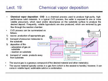
Lect. 19 Chemical vapor deposition
- Chemical vapor deposition (CVD) is a chemical
process used to produce high-purity,
high-performance solid materials. In a typical
CVD process, the wafer is exposed to one or more
volatile precursors, which react and/or decompose
on the substrate surface to produce the desired
deposit. Frequently, volatile byproducts are also
produced, which are removed by gas flow through
the reaction chamber.
- CVD process can be summarized as follows
- source production of appropriate gas
- transport of precursor molecules to the substrate
- deposition of film - adsorption of gas on
substrate - reaction on substrate - transport of "waste" products away from substrate
- The source gas is a gaseous compound of the
desired material and other material(s). - The source material typically comes in a gas form
(which is the easiest to handle,) however, it can
come in volatile liquid, sublimable solid or a
combination.
2
Chemical vapor deposition
Reaction chamber
- a The source gas (after interaction with a
reactive gas if any) flows to the substrate. - b The source precursors diffuse and adsorbed to
the surface of the substrate. (If a reactive gas
is used, at this point it is desorbed and flow
through the exhaust system) - c The precursors diffuse further across the
surface of the wafer. - d The precursors decompose incorporating to the
film material (chemical reaction). - e The volatile byproducts of the reaction on
the wafer surface are desorbed into a gas phase
and flow through the exhaust system. - To source material should be
- Stable at room temperature.
- Reaction temperatelt melting point of the
substrate. - Produce desired element on the substrate with
volatile byproducts. - Low toxicity.
gas out
gas in
heater
3
Chemical vapor deposition
- CVD reaction types
- Pyrolysis- Thermal decompositionAB(g) ?A(s)
B(g), ex Si deposition from Silane at 650 C
A desired material, B volatile
byproductSiH4(g) ? Si(s) 2H2(g) Use to
deposit Al, Ti, Pb, Mo, Fe, Ni, B, Zr, C, Si,
Ge, SiO2, Al2O3, MnO2, BN, Si3N4, GaN, - Reduction Often usingH2, AX(g) H2(g) ? A(s)
HX(g)A desired material, X reactive gas,
g gas, s solidOften require lower
temperature than pyrolysis and it is
reversible,hence can be used for cleaning
too.ex W deposition at 300 C, WF6(g) 3H2(g)
? W(s) 6HF(g) Used to deposit Al, Ti, Sn,
Ta, Nb, Cr, Mo, Fe, B, Si, Ge, TaB, TiB2, SiO2,
BP, Nb3Ge,. . . - OxidationOften using O2, AX(g) O2(g) ? AO(s)
OX(g) A desired material, X reactive
gas, g gas, s solid - ex SiO2 deposition from silane and oxygen at 450
C (lower temp than thermal oxidation)SiH4(g)
O2(g) ? SiO2(s) 2H2(g) Use to deposit Al2O3,
TiO2, Ta2O5, SnO2, ZnO, . . .
Reference http//www.uccs.edu/tchriste/courses/P
HYS549/549lectures/cvd.html
4
Chemical vapor deposition
- When using CVD for deposition, there are factors
regarding the substrate and the material to be
considered - Adsorption of the substrate to the source
material If the substrate material does not
adsorb the precursors then there will be no
growth. - The surface reactions, some materials react on
some substrates not others. For example WF6
deposits on Si but not on SiO2. - Hence, the film growth depends on the following
parameters - transport of gas to surface
- adsorption of gas on substrate
- reaction rates on substrate
- transport of the byproducts away from substrate
- Transport of gas to surface
- Deliver gas uniformly to substrate (uniform
films) - Optimize flow for maximum deposition rate
- Around the substrate, there are two types of
flowMolecular flow and viscous flow
Molecular flow
v
v
??
Substrate
Viscous flow
5
Chemical vapor deposition
- In the molecular flow case, or gas transport
limit, the molecules diffuse in gas with a
diffusivity,
, which can be derived from the kinetic
theory . - In the viscous flow, low flow rates produces
laminar flow (desired) while high flow rates
produces turbulent flow (avoid). - In the laminar flow, the gas molecule near the
surface has velocities approaching zero, hence we
can assume a stationary (stagnant) layer just
above the surface with thickness ?. - We will use the simple Groves model (like in the
thermal oxidation case) to estimate the
deposition rate in CVD. - Assume a Thermal decomposition reaction AB(g)
?A(s) B(g)
Gas flow
Stagnant layer
J1
??
J2
New film layer
Film
Substrate
6
Chemical vapor deposition
7
Lect. 20 Chemical vapor deposition
- There are two limiting cases
- If hg is small (D is small or?? is large) hence
. In this case the
deposition rate depends on the transfer of the
source gas to the surface (diffusion of the
molecules to the surface). - This case is referred to as mass transfer limited
8
Chemical vapor deposition
- hg is not very temperature dependent ? limit at
higher temperatures - The other limit is when ks is very small, or
surface reaction limit - Here, the growth is very much controlled by the
reaction of the gases on the surface of the
wafer- adsorption - decomposition - surface
migration - chemical reaction- desorption of
products - kS is highly temperature dependent
- common limit at lower temperatures which is
preferred - It is also a common limit at high gas flow rate,
v, where hg becomes much larger than ks.
Ref http//organics.eecs.berkeley.edu/viveks/ee1
43/lectures/section6p4.pdf
9
Chemical vapor deposition
- Types of CVD systems according to pressure
- Atmospheric pressure CVD (APCVD) - CVD processes
at atmospheric pressure (1 atm). - Nitrogen works as a curtain for the desired gas
flow. - The substrates can be fed continuously throw the
system. - It can handle large diameter wafers.
- Requires high gas flow rate.
- Low-pressure CVD (LPCVD) - CVD processes at
sub-atmospheric pressures (0.1 to 1 torr).
Reduced pressures tend to reduce unwanted
gas-phase reactions and improve film uniformity
across the wafer. - At low pressure, hg becomes large compared to ks
and the process is most likely to be surface
reaction limit - Gases are inserted from one end and pumped out
from the other end. - Can process hundreds of wafers at one run.
- It has the disadvantage of contamination as the
deposited material coats the tube and frequent
cleaning processes are rrequired.
APCVD
Hot wall LPCVD
Ref http//users.ece.gatech.edu/alan/ECE6450/Lec
tures/ECE6450L13and14-CVD20and20Epitaxy.pdf
10
Chemical vapor deposition
- The other type of CVD is Plasma-Enhanced CVD
(PECVD) - CVD processes that utilize a plasma to
enhance chemical reaction rates of the
precursors. PECVD processing allows deposition at
lower temperatures, which is often critical in
the manufacture of semiconductors. - In parallel plate PECVD, wafer lay on a grounded
aluminum serves as a buttom electrode. - The top electrode is parallel to the bottom one.
- Gases flow from the side and are pumped out
throw the exhaust in the center. - An RF signal is applied on the top electrode
toproduce plasma. - Wafers are loaded manually.
- Furnace plasma system can handle many wafers at
one time. - A special electrode assembly holds the
wafersparallel to the gas flow.
Parallel plates PECVD
Furnace PECVD
11
Chemical vapor deposition
- Silicon dioxide
- Silicon dioxide (usually called simply "oxide" in
the semiconductor industry) may be deposited by
several different processes. Common source gases
include silane and oxygen, dichlorosilane
(SiCl2H2) and nitrous oxide (N2O), or
tetraethylorthosilicate (TEOS Si(OC2H5)4). The
reactions are as follows - SiH4 O2 ? SiO2 2H2
- SiCl2H2 2N2O ? SiO2 2N2 2HCl
- Si(OC2H5)4 ? SiO2 byproducts
- The choice of source gas depends on the thermal
stability of the substrate for instance,
aluminium is sensitive to high temperature.
Silane deposits between 300 and 500 C,
dichlorosilane at around 900 C, and TEOS between
650 and 750 C. However, silane produces a
lower-quality oxide than the other methods (lower
dielectric strength, for instance), and it
deposits nonconformally. Any of these reactions
may be used in LPCVD, but the silane reaction is
also done in APCVD. CVD oxide invariably has
lower quality than thermal oxide, but thermal
oxidation can only be used in the earliest stages
of IC manufacturing. - Oxide may also be grown with impurities (alloying
or "doping"). This may have two purposes. During
further process steps that occur at high
temperature, the impurities may diffuse from the
oxide into adjacent layers (most notably silicon)
and dope them. Oxides containing 5 to 15
impurities by mass are often used for this
purpose. In addition, silicon dioxide alloyed
with phosphorus pentoxide ("P-glass") can be used
to smooth out uneven surfaces. P-glass softens
and reflows at temperatures above 1000 C. This
process requires a phosphorus concentration of at
least 6, but concentrations above 8 can corrode
aluminium. Phosphorus is deposited from phosphine
gas and oxygen - 4PH3 5O2 ? 2P2O5 6H2
12
Chemical vapor deposition
- Silicon nitride
- Silicon nitride is often used as an insulator and
chemical barrier in manufacturing ICs. The
following two reactions deposit nitride from the
gas phase - 3SiH4 4NH3 ? Si3N4 12H2
- 3SiCl2H2 4NH3 ? Si3N4 6HCl 6H2
- Silicon nitride deposited by LPCVD contains up to
8 hydrogen. It also experiences strong tensile
stress (physics), which may crack films thicker
than 200 nm. However, it has higher resistivity
and dielectric strength than most insulators
commonly available in microfabrication (1016 Ocm
and 10 MV/cm, respectively). - Another two reactions may be used in plasma to
deposit SiNH - 2SiH4 N2 ? 2SiNH 3H2
- SiH4 NH3 ? SiNH 3H2
- These films have much less tensile stress, but
worse electrical properties (resistivity 106 to
1015 Ocm, and dielectric strength 1 to 5 MV/cm).
13
Chemical vapor deposition
- Metals
- Some metals (notably aluminium and copper) are
seldom or never deposited by CVD. As of 2002, a
viable CVD process for copper did not exist, and
the metal was deposited by electroplating.
Aluminium can be deposited from tri-isobutyl
aluminium, but physical vapor deposition methods
are usually preferred. - However, CVD processes for molybdenum, tantalum,
titanium and tungsten are widely used. These
metals can form useful silicides when deposited
onto silicon. Mo, Ta and Ti are deposited by
LPCVD, from their pentachlorides. In general, for
an arbitrary metal M, the reaction is as follows - 2MCl5 5H2 ? 2M 10HCl
- The usual source for tungsten is tungsten
hexafluoride, which may be deposited in two ways - WF6 ? W 3F2
- WF6 3H2 ? W 6HF
Recommended
CrystalGraphics Presentations


