Nanoscale Electrochemical Switches - PowerPoint PPT Presentation
1 / 12
Title:
Nanoscale Electrochemical Switches
Description:
Nanoscale Crossbar Fabrication. Science 300 (2003) 112-115. State of the Art Filament Switches ... Fabricate nanoscale memory devices. Collaboration Opportunities ... – PowerPoint PPT presentation
Number of Views:61
Avg rating:3.0/5.0
Title: Nanoscale Electrochemical Switches
1
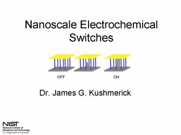
Nanoscale Electrochemical Switches
OFF
ON
- Dr. James G. Kushmerick
2
Nanoscale Electrochemical Switches
2 nm
OFF
ON
1. OFF state molecular tunnel junction 2.
Vthreshold reached. Ag filament bridges gap.
Switches ON. 3. Remains in ON state until
polarity switched. 4. At 0 V, device is returned
to OFF state.
Device can be rapidly cycled between ON and
OFF Greater than 1 million switch cycles
achieved Fastest monolayer switch to date 13
kHz On-Off Ratio gt 105 Device area 25 nm2
3
Detail of Switch Mechanism
4
Why would anyone be interested in a nanoscale
switch?
5
CMOS Scaling
65 nm node (2005)
drives Si technology towards fundamental limits
Courtesy of Intel
Rocks Law the cost of a semiconductor chip
fabrication plant doubles every four years
Courtesy INTEL
6
Nanoscale Crossbar Fabrication
Science 300 (2003) 112-115
7
State of the Art Filament Switches
8
Advantages
- Ease of fabrication
- Huge On-Off Ratio (gt105)
- High success rate for device fabrication (gt90)
- Small Device Area (25 nm2)
Challenges/Opportunities
- Slow Switch Speed (10 kHz) defines possible
applications (e.g. memory arrays and FPGA) - Not easily integrated into CMOS fab-line, but no
fab-line needed
9
Technology Applications
- Nanoscale Electrical Devices
- Memory Arrays
- Field-Programmable Gate Arrays
Commercial Applications
- Memory and logic for cell phone and other
portable electronic devices
10
Future Work
- Optimization of switch characteristics
- Increase switch speed
- Increase of cycles till failure
- Fabricate nanoscale memory devices
11
Collaboration Opportunities
- Future work would best be done in collaboration
between NIST and an interested industrial
partner. - Intellectual Property
- Self-Assembled Monolayer Based Silver Switches
- Provisional Patent Application filed 9/10/2007
- Serial 11/852,811
12
Contact Information
- For further information contact
- James G. Kushmerick100 Bureau Drive Stop
8372Gaithersburg, MD 20899-8372Tel (301)
975-5697email james.kushmerick_at_nist.gov


