Design Margining - PowerPoint PPT Presentation
1 / 7
Title:
Design Margining
Description:
Device characteristics follow normal distribution N(a, ) 2. 3. 1 =68.26% 2 =95.44% 3 =99.74 ... Device failure/degradation. Hot electron effect ... – PowerPoint PPT presentation
Number of Views:55
Avg rating:3.0/5.0
Title: Design Margining
1
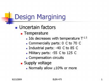
Design Margining
- Uncertain factors
- Temperature
- Ids decreases with temperature T-1.5
- Commercially parts 0C to 70C
- Industrial parts -40C to 85C
- Military parts -55C to 125C
- Compensation circuits
- Supply voltage
- Normally allow ?10 or more
2
Process Variation
- Device characteristics follow normal distribution
N(a, ?)
3?
1? 68.26 2? 95.44 3? 99.74
2?
Device char within 3? is reported as variation
?
3
Process Variation
- Device
- Gate length
- Oxide thickness
- Doping density
- Interconnect
- Metal width, metal thickness
- Inter-layer-dielectric thickness
- Via resistance
4
Impact of Process Variation
- Delay variation wafer-to-wafer, chip-to-chip,
region-to-region, or random
5
Delay Fault
- Path delay fault
- Path delay is d
- Process variation causes extra delay ?
- If d ?gtTcycle, then there is a delay fault
To POs or FFs
From PIs or FFs
P1
P1
P2
P2
Combinational Circuit
T
cycle
6
Design Corners
- Imaginary box that surrounds the guaranteed
performance - For example, when all devices on one path has
longest gate length, while all devices on another
path has shortest gate length - Rarely happen, but can be a problem
- Verification and testing
7
Reliability
- Device failure/degradation
- Hot electron effect
- Electromigration
- Oxide failure
- Transistor degradation
- Accelerated life testing
- Over-voltage, over-temperature

