Full wave CenterTapped transformer - PowerPoint PPT Presentation
1 / 20
Title:
Full wave CenterTapped transformer
Description:
PIV 2Vm for ideal diode and PIV 2Vm 0.7 for practical model ... The effect of using a silicon diode with VT: The dc level will change to: ... – PowerPoint PPT presentation
Number of Views:1685
Avg rating:3.0/5.0
Title: Full wave CenterTapped transformer
1
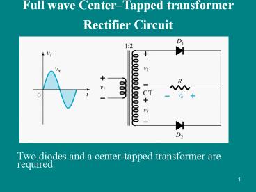
Full wave CenterTapped transformer Rectifier
Circuit
Two diodes and a center-tapped transformer are
required.
2
Operation of the CenterTapped Transformer
Rectifier Circuit
For the positive half of the AC
cycle For the negative half of the AC
cycle
3
- No matter the value of the turns ratio the
output is always for ideal
diode - or for
practical model - Where Vsec is the end to end voltage of the
secondary transformer winding - PIV gt2Vm for ideal diode and PIV gt2Vm 0.7 for
practical model - Note that Vm here is the transformer secondary
voltage to the tap. - VDC 0.636(Vpout) (since the area above the axis
is double the area obtained for the half wave
rectifier) - Ir.m.sIpout/v2
4
Example
- Show the voltage waveforms across each half of
the secondary winding and across RL when a 100 V
peak sine wave is applied to the primary winding.
Also, what PIV rating must the diodes have?
5
- Each diode must have a minimum PIV rating of 50
V (neglecting diode drop). The waveforms are
shown in Figure
6
Full-Wave RectificationBridge Network
- The dc level obtained from a sinusoidal input can
be improved 100 using a process called full-wave
rectification. - The most familiar network is bridge configuration
with 4 diodes.
7
Operation of the Bridge Rectifier Circuit
For the positive half of the AC cycle
For the negative half of the AC cycle
8
FULL WAVE RECTIFICATION
- The rectification process can be improved by
using more diodes in a Full Wave Rectifier
circuit. - Full Wave rectification produces a greater DC
output.
9
(No Transcript)
10
Example
- Determine the output voltage for the bridge
rectifier in Figure . What PIV rating is required
for the silicon diodes? The transformer is
specified to have a 12 V rms secondary voltage
for the standard 110 V across the primary.
11
Solution
- The peak output voltage is (taking into account
the two diode drops) - VPsec 1.414Vrms 17 V
- VPout VPsec -1.4 15.6V
- The PIV for each diode is
- PIVVPout 0.7V15.6V0.7V16.3V
12
POWER SUPPLY FILTERS(PEAK DETECTORS)
- The pulsating dc output of a half-wave rectifier
or the output of a full-wave rectifier must be
filtered to reduce the large voltage variations.
The figure below illustrates the filtering
concept showing a nearly smooth dc output voltage
from the filter. The small amount of fluctuation
in the filter output voltage is called ripple.
13
Capacitor Filter
- A half-wave rectifier with a capacitor filter is
shown in Figure . RL represents the equivalent
resistance of a load. We will use the half-wave
rectifier to illustrate the principle, and then
expand the concept to full-wave rectification. - During the positive first quarter-cycle of the
input, the diode is forward-biased , allowing the
capacitor to charge to within 0.7 V of the input
peak.
14
- When the input begins to decrease below its peak,
as shown in part (b), the capacitor retains its
charge and the diode becomes reversebiased.
During the remaining part of the cycle, the
capacitor can discharge only through the load
resistance at a rate determined by the RLC time
constant, which is normally long compared to the
period of the input.
15
- The larger the time constant, the less the
capacitor will discharge. During the first
quarter of the next cycle, the diode will again
become forward-biased when the input voltage
exceeds the capacitor voltage by approximately
0.7 V. - The variation in the output voltage due to the
charging and discharging is called the ripple
voltage. - The smaller the ripple, the better the filtering
action
16
- For a given input frequency, the output frequency
of a full-wave rectifier is twice that of a
half-wave rectifier. This makes a full-wave
rectifier easier to filter. - The full-wave rectified voltage has a smaller
ripple than does a half-wave voltage for the same
load resistance and capacitor values.
17
Ripple Factor
- The ripple factor is an indication of the
effectiveness of the filter and is defined as - where Vr is the peak-to-peak ripple voltage and
VDC is the dc value of the filter's output
voltage. - The lower the ripple factor, the better the
filter. The ripple factor can be lowered by
increasing the value of the filter capacitor or
increasing the load resistance.
18
- For a full-wave rectifier with a sufficiently
high capacitance filter, if VDC is within 10 of
the peak rectified input voltage, then the
expressions for the peak-to-peak ripple voltage,
Vr and VDC are as follows - where Vp(in) is the peak rectified full-wave
voltage applied to the filter - and f is 60 (50) Hz for a half-wave rectifier or
120(100) Hz for a full-wave rectifier
19
Example
- Determine the ripple factor for the filtered
bridge rectifier .
20
(No Transcript)

