
MPW Design Introduction Course Part 5 - PowerPoint PPT Presentation
1 / 19
Title:
MPW Design Introduction Course Part 5
Description:
BOGEB mirrored! Relatively high line-width. 15. Die lay-out rules (1) Metal line contacts epi across entire die: uniform potential distribution during ... – PowerPoint PPT presentation
Number of Views:67
Avg rating:3.0/5.0
Title: MPW Design Introduction Course Part 5
1
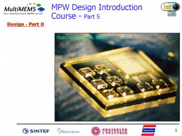
MPW Design Introduction Course - Part 5
Design - Part II
2
Contents Design- Part II
- Masks description Pressure sensor example
- Die lay-out rules
3
NOWEL mask (N-well)
- Straight polarity
- n-well implant in clear area
- No implant in the area to be dry etched
4
BUCON mask(buried conductors)
- Reverse polarity
- B implant in dark area
- Inter-layer rules
- NOWEL
5
BURES mask(buried resistors)
- Reverse polarity
- B-implant in dark area
- Note SURES also
- Inter-layer rules
- BUCON, NOWEL
6
TIKOX mask (thick oxide)
- Straight polarity
- Insulating oxide between Si and metal
7
SUCON mask (surface conductor)
- Reverse polarity
- B-implant in dark area
- Inter-layer rules
- BUCON, NOWEL
- BURES, TIKOX
8
NOSUR mask (N-layer)
- Straight polarity
- P-implant in clear area
- Inter-layer rules
- BUCON, BURES
- TIKOX
9
COHOL MCOND masks (contact holes and metal)
- Reverse / straight
- Inter-layer rules
- NOSUR, TIKOX
- COHOL, MCOND,
- SUCON, BUCON
10
BETCH mask (backside etch)
11
NOBOA mask (anodic bonding area)
- Straight polarity
- Inter-layer rules
- SUCON, SURES
12
RETCH mask (release etch)
- Separate example !!
- Reverse polarity
- Inter-layer rules
- SUCON, SURES
- MCOND, TIKOX
13
TOGE mask (top glass etch)
- Reverse polarity
- Mirrored!
TOGE
14
BOGEF BOGEB masks (bottom glass etch)
- Reverse polarity
- BOGEB mirrored!
- Relatively high line-width
15
Die lay-out rules (1)
Metal line contacts epi across entire die
uniform potential distribution during anisotropic
etching crossing over buried conductors thick
oxide
16
Die lay-out rules (2)
- The bond pads area to the right of the chip
- Pitch and size of bond pads (no rule)
- Min. 120 µm wide anodic bonding area
17
Die lay-out rules (3)
- Connection between bond pads and active area
buried conductors - Top glass etched over the bond pad area
- Note also substrate contact (not a rule)
18
Summary
19
Ch 5 Design Part II
- End of this chapter
- Questions or comments?
Recommended
CrystalGraphics Presentations


