Roadmap of Microelectronic Industry - PowerPoint PPT Presentation
1 / 19
Title:
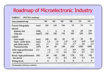
Roadmap of Microelectronic Industry
Description:
Armchair (n, n) Zigzag (n, 0) General (m, n) Electronic properties of SWNTs ... Armchair, dt = 1.4nm. STM I-V spectroscopy. Bandgap of semiconducting SWNTs: ... – PowerPoint PPT presentation
Number of Views:98
Avg rating:3.0/5.0
Title: Roadmap of Microelectronic Industry
1
Roadmap of Microelectronic Industry
2
Scaling of MOSFET
Reduction of channel length L ? L/a
Integration density ? a2 Speed ? a
Power/device ? 1/a2 Power density unchanged
Voltage ? 1/a Equivalent thickness of gate
oxide ? 1/?
3
Gate Dielectric film in ULSI MOSFET
Gate oxide
Gate
n
n
p-Si
4
Equivalent Gate Oxide ThicknesstEq tx
?SiO2/?x ?x dielectric constant of insulator
X ?SiO2 3.2 Use high-?x insulator
5
Possible epitaxial dielectric films on Si
6
Metallization target parameters
(current)
7
Electromigration Effects
Void Pile-up
Electron wind and field-driven atomic migration
8
Multi-level Metallization
RC delay issue
Lower levels fine connections to individual
devices Upper levels thicker/wider common
connections Cu metallization reducing wire
resistance Low-k dielectrics reducing parasitic
capacitance
9
Lithography shorter wavelength (deep UV, X-ray,
electron/ion beams) source, optics, resist
materials
Gate insulator with high dielectric constant
(high-k), high dielectric strength, effective
barrier to impurity (e.g., B) migration
Si-on-insulator (SOI) reducing capacitive
coupling between devices, power consumption,
effective heat dissipation
10
Double-gate FET
Double-gate FET by selective epitaxial growth
11
Single-electron Tunneling (SET)
Transistor Coulomb blockade effect
Devices based on quantum effects in
nano-structured materials quantum dots/wire,
nano-wires (e.g., carbon nanotubes), molecular
devices,
12
Index of Single-wall Carbon Nanotubes (SWNT)
Armchair (n, n) Zigzag (n, 0) General (m, n)
13
Electronic properties of SWNTs
SWNTs 1D crystal If m - n 3q ? metallic
Otherwise ? semiconductor
Zigzag, dt 1.6nm
?18?, dt 1.7nm
Bandgap of semiconducting SWNTs
?21?, dt 1.5nm
?11?, dt 1.8nm
Armchair, dt 1.4nm
1.42 Å, ? 5.4 eV, overlap integral
STM I-V spectroscopy
14
Doping of semiconductor SWNTs N, K atoms ?
n-type B atoms, oxygen ? p-type
SWNT Transistors
SWNT CMOS inverter its characteristics
15
Molecular diodes and nonlinear devicesMolecule
with D-?-A structure C16H33Q-3CNQ
D
?
A
Highly conductive zwitterionic D-?-A- state at
1-2V forward bias Reverse conduction state
D--?-A requires bias of 9V I-V curve of Al/4-ML
C16H33Q-3CNQ LB film/Al structure
16
Ultimate Physical Limits
Thermodynamic limit energy consumption in
handling 1 bit of information kT log 2 ? 18 meV
3 ? 10-21 J at RT Current products Pentium
4, power consumption 30 W, consists gt 2.5 ? 106
devices operating at gt 4 ? 108 Hz, energy cost
per bit of operation ? 10-15 J Demonstrated in
laboratory energy cost of operating a
single-molecule switch is 10-19 J
17
Real Materials and their Processing
- Particles, lines and rigid bodies vs. real
materials each material has its own
characteristics - Material-specific properties determine the
function and processing details of a material - Comprehensive knowledge of materials processing
requires 5-10 years of learning and practice
Interdisciplinary between physics, chemistry,
electronics, materials science, economics - Advantage and role of physicist
18
Graduate Attributes (Southern Cross University,
Australia)
- Intellectual rigour
- Creativity
- Ethical understanding, sensitivity, commitment
- Command an area of knowledge
- Lifelong learning --- ability of independent
self-directed learning - Effective communication and social skills
- Cultural awareness
- (From S. Yeo, CDTLink, NUS, July 2004)
19
Final Exam
- 24 Nov, two hours
- One A4 cheat sheet allowed, both sides
- What will be in the exam?
- Basic principle, processes, mainly after
Chapter 5


