MESFET models - PowerPoint PPT Presentation
1 / 19
Title:
MESFET models
Description:
unity short-circuit current gain frequency fT. unity power gain fmax ... T. Block, T.P. Chin, V. Medvedev, E. Sabin, H. Rogers, P. H. Liu, Y.C. Chen, R. ... – PowerPoint PPT presentation
Number of Views:1804
Avg rating:3.0/5.0
Title: MESFET models
1
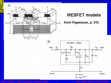
MESFET models
- from Yngvesson, p. 313.
2
Simple limits
- simple results
- unity short-circuit current gain frequency fT
- unity power gain fmax
- from Sze, High Speed Devices
3
Velocities
- steady state
- ballistic for short channels
- from Yngvesson
4
Saturation condition
- from C. Liechti, Microwave Field-Effect
Transistors 1976, IEEE Trans. Micro. Theory
Tech., MTT-24, p. 279, 1976.
5
Channel resistance term Ri
- from Ladbrooke, MMIC Design GaAs FETs and HEMTs,
p. 100,
6
Ri term
- from Ladbrooke, MMIC Design GaAs FETs and HEMTs.
7
breakdown limits
- from Sze, High Speed Devices
8
RF cmos trends
- from RF-CMOS Performance Trends, Pierre
H.Woerlee, Mathijs J. Knitel, Ronald van
Langevelde, Dirk B. M. Klaassen, Luuk F.
Tiemeijer, Andries J. Scholten, and Adrie T. A.
Zegers-van Duijnhoven, IEEE TRANSACTIONS ON
ELECTRON DEVICES, VOL. 48, NO. 8, AUGUST 2001,
pp. 1776-1782
Fig. 1. Measured f data of nominal gate length
NMOS devices from industrial CMOS technologies
versus minimum feature size. solid square
Philips, open triangle E. Morifuji, H. S.
Momose, T. Oghuro, T. Yoshitomi, H. Kimijima, F.
Matsuoka, M. Kinugawa, Y. Katsumata, and H. Iwai,
Dig. Tech. Papers VLSI Symp., 1999, p. 163.
closed triangle T. C. Holloway et al., Dig.
Tech. Papers VLSI Symp., 1997, p. 13. open
diamond J. N. Burghartz et al., IEDM Tech. Dig.,
1999, p. 853.).
9
MOSFET models
- from http//www.planetanalog.com/story/OEG20001024
S0010
10
Silicon - germanium
- from Monte Carlo Investigation of Optimal Device
Architectures for SiGe FETs, S. Roy, S. Kaya, S.
Babiker, A. Asenov, J. Baker, http//www.elec.gla.
ac.uk/groups/dev_mod/papers/iwce98/SiGe.pdf
11
Si-Ge fets
- from The Future of SiGe Beyond HBT Applications,
Dr. Thomas Hackbarth, Dipl. Ing. Marco Zeuner,
Dipl. Ing. and Dr. Ulf König, DaimlerChrysler
Research Center, Ulm, Germany, http//www.semicond
uctors.unaxis.com/en/download/The20Future20of20
SiGe.pdf - e Beyond HBT Applications, Dr. Thomas Hackbarth,
Dipl. Ing. Marco Zeuner, Dipl. Ing. and Dr. Ulf
König, DaimlerChrysler Research Center, Ulm,
Germany, http//www.semiconductors.unaxis.com/en/d
ownload/The20Future20of20SiGe.pdf
12
High Electron Mobility Transistor
- AKA
- heterojunction fet (HFET)
- modulation-doped FET, MODFET
- two-dimensional electron gas FET, 2DFET, TEGFET
- first device 1980
- Gate delays as low as 12 psec at room temperature
(1984) - At 77 K saturation velocities twice
conventional MESFET. - essentially achieve mobility of undoped GaAs in
channel - requires for fabrication
- MBE to grow both GaAs and AlxGa1-xAs
- sub-micron gate definition
- implantation for contacts
13
Basic idea
- GaAs and AlGaAs are latticed matched throughout
their compositional range
from Sze, High Speed Semiconductor Devices, p.
285.
from Sze, High Speed Semiconductor Devices, p.
290.
14
Device structure
- critical parameters
- doping concentration in AlGaAs
- want fully depleted, as many carriers in channel
as possible - spacer layer thickness
- want to minimize scattering from ionised
impurities - still want max channel sheet carrier concentration
from Sze, High Speed Semiconductor Devices, p.
285, 300.
15
Results
from Sze, High Speed Semiconductor Devices, p.
297, 299, 298.
16
Other materials
- look for
- higher low field mobility
- higher velocities
- main issue
- can you grow the material?
from Sze, High Speed Semiconductor Devices, p.
301.
17
InGaAs hemts
- from 0.1 µm InGaAs/InAlAs/InP HEMT Production
Process for High Performance and High Volume MMW
Applications, - R. Lai, M. Barsky, R. Grundbacher, L. Tran, T.
Block, T.P. Chin, V. Medvedev, E. Sabin, H.
Rogers, P. H. Liu, Y.C. Chen, R. Tsai and D.
Streit, TRW Inc., Electronic Systems and
Technology Division http//www.gaasmantech.org/dig
est/1999/PDF/16.pdf
18
AlGaN/GaN
- higher breakdowns GaN Egap 3.4eV breakdown
field 3MV/cm - higher powers more than higher fmax
- AlGaN/GaN MODFET record output power density of
3W/mm at 18GHz and 5.3W/mm at 10GHz 2 - T.S.Sheppard at al.,"High power microwave
GaN/AlGaN HEMTs on Silicon Carbide", in Late News
1998 56th Annual Device Research Conference,
avail. at http//schof.colorado.edu/drc/drc1998/l
ateprog.htm
from U.K. Mishra, P. Parikh, Y.F. Wu, AlGaN/GaN
HEMTs An overview of device operation and
applications, http//my.ece.ucsb.edu/mishra/cla
ssfiles/overview.pdf
19
SiGe hemts
from D.J. Paul, Silicon Germanium
Heterostructures in Electronics- The Present and
the Future, Thin Solid Films (Accepted for
publication)

