Laboratory - PowerPoint PPT Presentation
1 / 4
Title:
Laboratory
Description:
PC with Digital Storage Oscilloscope attachment ... Review operational amplifiers in Nilsson and Riedel. Op Amps are also covered in Chapter 14 of our textbook. ... – PowerPoint PPT presentation
Number of Views:61
Avg rating:3.0/5.0
Title: Laboratory
1
Laboratory 4
Corrected Version
Digital-to-Analog and Analog-to-Digital Converters
In this lab you will build and test several basic
DAC and ADC circuits.
- Equipment
- Knight Electronics Minilab with connecting wires
- Digital Multimeter
- PC with Digital Storage Oscilloscope attachment
- 1 of 15kW, 2 of 30kW, 3 of 60kW , and 1 of
120kW resistors - Operational amplifier
- Preparation
- Review operational amplifiers in Nilsson and
Riedel. Op Amps are also covered in Chapter 14 of
our textbook.
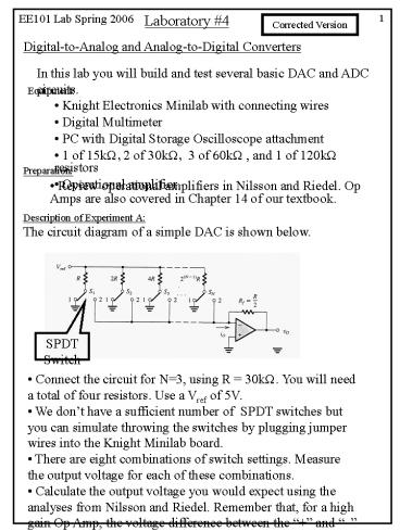
Description of Experiment A The circuit diagram
of a simple DAC is shown below.
SPDT Switch
- Connect the circuit for N3, using R 30kW. You
will need a total of four resistors. Use a Vref
of 5V. - We dont have a sufficient number of SPDT
switches but you can simulate throwing the
switches by plugging jumper wires into the Knight
Minilab board. - There are eight combinations of switch settings.
Measure the output voltage for each of these
combinations. - Calculate the output voltage you would expect
using the analyses from Nilsson and Riedel.
Remember that, for a high gain Op Amp, the
voltage difference between the and
terminals on the op amp will approach zero when a
resistor is connected between the output terminal
and the terminal. Therefore, it is
straightforward to calculate i0 and then v0.
2
Corrected Version
- Compare the calculated values of v0 to those you
measured. - You will very likely see some error. Precision
resistors would be used in a real DAC. - Use the digital multimeter to measure each
resistor and recalculate v0. You should now have
very good agreement between the measurements and
the calculations. - Make a plot showing v0 versus the digital input
(x-axis) for the three cases - Original calculations
- Measured values
- Calculations using measurements of each
resistor. - Explain the differences
- Description of Experiment B
- The DAC can be used as the basis for an Analog to
Digital Converter (ADC) as shown to the right. - Use the DAC you built in Experiment A. Keep
vref 5V. - Use the digital multimeter as a voltage
comparator. Attach the positive terminal of the
multimeter to the vin terminal. When vin gt vo,
the multimeter shows a positive voltage and vice
versus. - You can provide the functions performed by the
control circuits by observing the polarity of the
feedback voltage from the comparator and then
throwing the appropriate switches.
- The final position of the switches indicates the
digital output. - The control sequence uses a binary search and
you can proceed as follows - First calibrate the system by setting all the
switches at the 1 position. The output voltage
should be zero. - Next set all the switches at the 2 position.
The output voltage should be at the maximum
level, vmax which you measured in Experiment A.
3
Corrected Version
- Reset all the switches to the 1 position.
Throw the switch for the most significant digit
from the 1 to the 2 position. This will swing
the output voltage from zero to about ½ the
maximum voltage you measured above with all
switches at the 2 position. - If the voltage comparator reads a positive
value, we know that vin is greater than this
voltage. This means that the most significant
digit is 1. - Conversely, if the voltage comparator reads a
negative value, we know that vin is less than
approximately vmax/2. If this is the case, throw
the switch back to the 1 position. This tells
you that the most significant digit is 0. - Next proceed to the next significant bit and
repeat the sequence. - Then proceed to the third significant bit.
- The settings of the switches now tell you the
digital value of vin.
- The Lab Instructor will provide you an unknown
voltage to measure. - Please use the ADC to measure the unknown
voltage first. - After you have measured the digital value of
the unknown voltage, calculate the decimal value.
- Then use the digital multimeter to measure the
unknown. - Compare the results.
- How much error do you have?
- Explain the sources of the error? What is the
effect of having a three bit DAC rather than a
12 bit DAC.
Description of Experiment C
The DAC in experiment A requires a wide range of
resistor values. For a 12 bit DAC, the resistor
range would be 213/1 8192/1. This is difficult
to manufacture to high accuracy. Therefore, the
more practical implementation is the ladder
network shown below.
4
Corrected Version
- Connect up this circuit with R 30kW. Use R/2
for the feedback resistor of the Op Amp. - Repeat the measurements made in Experiment A.
- Compare the results to those of Experiment A.
- Lab Report
- Follow the guidelines given for the earlier labs
- Be sure to clearly document all of your
measurements, observations and conclusions.


